3-D MID / Film Technology

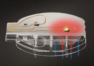
| Heat Sink with Conductor and LED |
To date three-dimensional injection-molded circuit carriers have been called Molded Interconnect Devices (3D MID for short). These combine electrical and mechanical elements into one part. The production of the component is followed by the application of the conductive paths and the assembly. Thereby, in contrast to conventional two-dimensional circuit board-technology, completely new approaches in design and functionality can be taken. Furthermore, the process chain is shortened and thermal transition regions are reduced. Instead of using traditional thermoset materials in electronics, technical thermoplastics (e.g. PA, PBT, PC and ABS) and High-Temperature-thermoplastics (e.g. PPS, PEI, PES or LCP) are used as a substrate material. Having overcome the limitations of traditional thermoset materials, it has become evident, that the term “MID” expands more and more to Mechatronic Integrated Devices. This extends to the fact, that components no longer need to be manufactured via plastic injecting molding. Rather, other materials like ceramics are beeing incorporated. MID production can occur with different processing types depending on the metallization and structuring of the component. Research at “Lehrstuhl für Kunststofftechnik” is focused on hot stamping, radiation-crosslinked plastics, laser structured surfaces, flexible circuit carriers based on plastic films and functionalization of plastics with fillers, e.g. in terms of electrical and thermal properties.
Research focuses are:
- Hot Stamping
- Development of new materials systems for laser direct structuring (LDS)
- Reliability of conductor structures
- Use of cross-linked plastics to increase temperature stability
- Flexible circuit carriers based on plastic films
Dr.-Ing. Uta Rösel
Institute of Polymer Technology
Processing (Head of Department)
- Phone number: +49913185-71002
- Email: uta.ur.roesel@fau.de
